


QR код

За нас
Производи
Контактирајте не


Факс
+86-579-87223657

Е-пошта

Адреса
Wangda Road, улица Ziyang, Wuyi County, Jinhua City, провинција Жеџијанг, Кина


Vetek Semiconductor е водечки производител на порозна SIC керамика за индустријата за полупроводници. Поминат ISO9001, Vetek полупроводникот има добра контрола врз квалитетот. Полупроводникот на Ветек отсекогаш бил посветен да стане иноватор и лидер во порозната керамичка индустрија SIC.

Порозен керамички диск
Порозна керамика на SIC е керамички материјал што се отпушта на високи температури и има голем број меѓусебно поврзани или затворени пори внатре. Познато е и како микропорозна вакуумска чаша за вшмукување, со големини на пори кои се движат од 2 до 100ум.
Порозната керамика на SIC се користи во металургија, хемиска индустрија, заштита на животната средина, биологија, полупроводник и други полиња. Порозна керамика SIC може да се подготви со метод на пенење, метод на сол гел, метод на леење на лента, метод на цврсто тонење и метод на пиролиза на импрегнација.

Подготовка на порозна керамика Sic со метод на топење
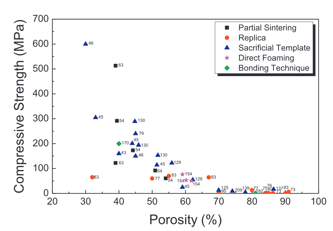
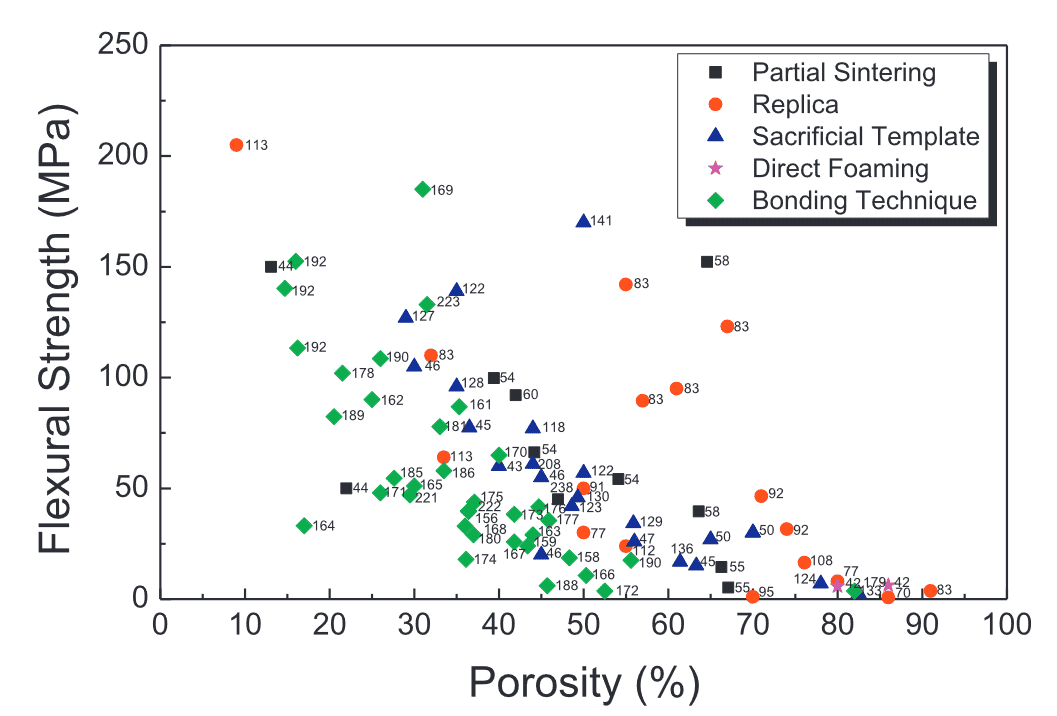
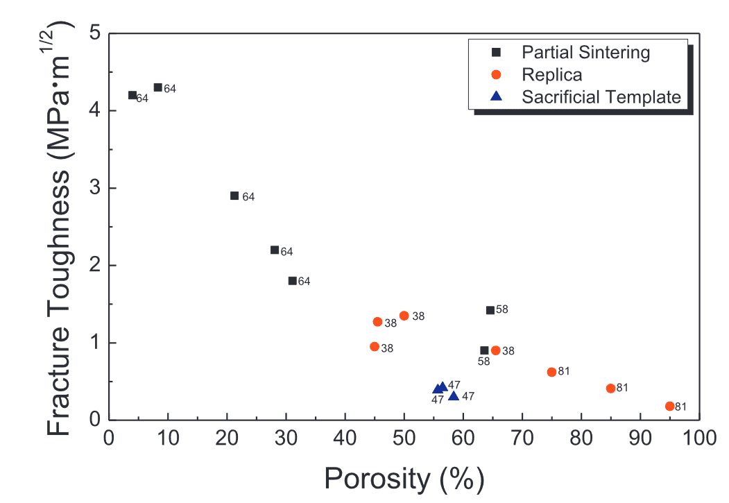
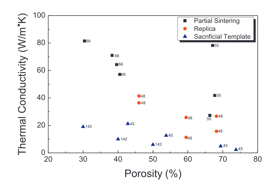
Карактеристики на порозна керамика на силиконски карбид подготвени со различни методи како функција на порозност

Порозни SIC керамика чаши за вшмукување во изработка на нафта на полупроводници
Порозната керамика на Vetek Semiconductor ја игра улогата на стегање и носење нафора во производството на полупроводници. Тие се густи и униформни, богати со сила, добра во пропустливост на воздухот и униформа во адсорпцијата.
Тие ефикасно се осврнуваат на многу тешки проблеми, како што се вовлекување на нафта и електростатско распаѓање на чипови и помагаат во постигнување на обработка на екстремно квалитетни нафори.
Работен дијаграм на порозна SIC керамика:

Работен принцип на порозна керамика Sic: Силиконскиот нафта е фиксиран со принципот на адсорпција на вакуум. За време на обработката, малите дупки на порозната керамика SIC се користат за да се извлече воздухот помеѓу силиконскиот нафта и керамичката површина, така што силиконскиот нафта и керамичката површина се на мал притисок, а со тоа да се поправи силиконскиот нафора.
По обработката, водата во плазмата излегува од дупките за да се спречи силиконскиот нафта да се придржува кон керамичката површина, а во исто време, силиконските нафора и керамичката површина се чистат.

Микроструктура на порозна керамика Sic
Означете ги предностите и карактеристиките:
● Отпорност на висока температура
● Отпорност на абење
● Хемиски отпор
● Висока механичка јачина
● Лесно се регенерира
● Одлична отпорност на термички шок
ставка
единица
Порозна SIC керамика
Дијаметар на пори
Еден
10 ~ 30
Густина
g / cm3
1.2 ~ 1.3
Површинска ругhness
Еден
2,5 ~ 3
Вредност на апсорпција на воздухот
Kpa
-45
Флексурална сила
МПА
30 Диелектрична константа
1MHz
33 Термичка спроводливост
W/(m · k)
60 ~ 70
Постојат неколку високи барања за порозна керамика на SIC:
1. Силна вакуумска адсорпција
2. Рамливоста е многу важна, во спротивно ќе има проблеми за време на работењето
3. Нема деформација и нема метални нечистотии
Затоа, вредноста на апсорпцијата на воздухот на порозната керамика на Vetek Semiconductor достигнува -45kpa. Во исто време, тие се смируваат на 1200 ℃ за 1,5 часа пред да ја напуштат фабриката за да ги отстранат нечистотиите и се спакувани во вакуумски кеси.
Порозната керамика на SIC се користи во технологијата за обработка на нафта, трансфер и други врски. Тие остварија големи достигнувања во сврзување, дигирање, монтирање, полирање и други врски.


Order precision-engineered Porous SiC ceramics from Veteksemicon—ideal for thermal uniformity and gas control in semiconductor systems.
Veteksemicon’s porous silicon carbide (SiC) components are engineered for high-temperature plasma processes and advanced gas flow control. Ideal for PECVD, ALD, vacuum chucks, and gas distribution plates (showerheads), these components offer excellent thermal conductivity, thermal shock resistance, and chemical stability.
Our porous SiC features a controlled pore structure for consistent gas permeability and uniform temperature distribution, reducing defect rates and enhancing yield. It is widely used in wafer handling platforms, temperature equalizing plates, and vacuum holding systems. The material ensures mechanical durability under corrosive and high-load thermal conditions.
Contact Veteksemicon today to request custom Porous SiC solutions or detailed engineering parameters.
+86-579-87223657
Wangda Road, улица Ziyang, Wuyi County, Jinhua City, провинција Жеџијанг, Кина